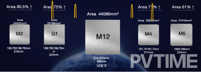
CHANGCHUN, CHINA, February. 5, 2019 /PVTIME/ – The biggest focus of the silicon wafer market in 2019 was the launch of 210mm large-size silicon wafer. The G12 wafer(initially named M12), has an 80.5% increase in surface area than the original 8-inch M2 wafer, a 75% increase over the G1 (158.75mm) wafer, a 71% increase over the M4 (161.7mm) wafer, and a 61% increase when compared to the M6 (166mm) wafer, will reduce the LCOE and increase manufacturing enterprises’ profits.
The market has been anticipating the arrival of large-size silicon wafer but the timetable for mass-production of these wafers has always been the main concern. Since the release of Zhonghuan Semiconductor’s 12-inch ultra-large “Kuafu” G12 series silicon wafers, Zhonghuan’s operation layout and marketing promotion efforts to increase market share have become the focus of the market. At the same time, the market is also carefully observing the actions of other companies along the supply chain including cell and module manufacturers.
Aikosolar’s plan to mass-produce 5GW of 210mm high-efficiency solar cells, Risen Energy’s introduction of their 500W high-efficiency modules using 210mm silicon wafers, and GCL Poly’s announcement to produce 210mm monocrystalline wafers, the presence and advancement pace of the 210mm wafer has far exceed expectations.
On February 4, an investor asked on a Chinese investor relations platform, “When will Zhonghuan Semiconductor’s 210mm silicon wafers achieve mass-production?” and received this response from the Board Secretary of Zhonghuan Semiconductor (SZ002129), “the fifth phase of the project has been put into production, and the first batch of G12 monocrystalline silicon ingots were produced in December 2019. Since the release of G12 products, many clients have reached out with cooperation proposals. Presently, production orders for 2020 are largely filled. The gradual completion of the project’s fifth-phase will further highlight the photovoltaic industry’s competitive advantages over other forms of energy.”


